logo
Good price  online

products details

Created with Pixso. Home Created with Pixso. Products Created with Pixso.
Single Crystal Substrates
Created with Pixso. Maximum Size 4 Inch Diameter Single Crystal Substrates Mineralogical Garnet Test Report Provided Material for Technology

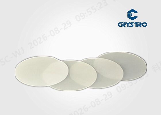
Maximum Size 4 Inch Diameter Single Crystal Substrates Mineralogical Garnet Test Report Provided Material for Technology

Brand Name: Crystro
Model Number: SGGG
Detail Information
Place of Origin:
China
Application:
Epitaxial Growth Of YIG,BIG Film
Polish:
EPI Polished Or Double Polished
Maximum Size:
4 Inch Diameter
Dia:
Up To 4''
Chemical Formular:
Substituted GGG
Lattice Constant:
12.497 ± 0.003 Å
Type:
Cubic/Round
Test Report:
Provided
Highlight:

4 inch garnet single crystal substrates

,

mineralogical garnet substrates with test report

,

technology material single crystal substrates

Product Description

Product Description:

Our Single Crystal Substrates are precision-engineered materials designed to meet the demanding requirements of advanced technological applications. These substrates are manufactured using substituted GGG (Gadolinium Gallium Garnet), which ensures exceptional crystalline quality and performance. With a 3inch diameter, these magneto-optical substrates are ideal for a wide range of optical and electronic devices, providing a robust platform for innovation and development.

One of the key features of our Single Crystal Substrates is their high lattice constant, which plays a crucial role in ensuring superior compatibility with various thin film materials. This high lattice constant minimizes lattice mismatch, thereby reducing defects and enhancing the overall performance of devices built on these substrates. This attribute makes them especially suitable for applications in magneto-optical devices, where precision and reliability are paramount.

We understand the importance of dimensional accuracy in substrate materials. Therefore, our Single Crystal Substrates come with a length tolerance of ±0.2mm, ensuring that each piece meets stringent specifications. This tight tolerance is critical for applications requiring exact dimensions to maintain the integrity and functionality of the final device. Additionally, we offer customized angle direction options, allowing customers to tailor the substrate orientation to their specific requirements. This customization capability enhances the versatility of our substrates for specialized research and industrial applications.

Another significant advantage of our Single Crystal Substrates is their dielectric constant of 30. This property is vital for applications involving high-frequency electronic components and microwave devices, where dielectric performance directly impacts device efficiency and signal integrity. The stable and predictable dielectric constant of our substrates ensures consistent performance across various operating conditions.

To provide our customers with confidence in the quality and reliability of our products, each batch of Single Crystal Substrates is accompanied by a comprehensive test report. This report verifies critical parameters such as dimensional accuracy, crystallographic orientation, dielectric properties, and surface quality. The availability of detailed test documentation supports quality assurance processes and facilitates smooth integration into manufacturing workflows.

Our Single Crystal Substrates are widely used in the fabrication of magneto-optical devices, optical isolators, modulators, and other advanced photonic components. The combination of a 3inch diameter size, high lattice constant, and excellent dielectric properties makes these substrates an excellent choice for researchers and manufacturers aiming to achieve high performance and reliability in their products.

In summary, our Single Crystal Substrates offer a unique combination of high-quality substituted GGG material, precise dimensional control, customizable orientation, and superior dielectric characteristics. Whether you are developing next-generation magneto-optical devices or exploring new frontiers in photonics and electronics, our substrates provide a dependable foundation to support your innovation. With comprehensive test reports and stringent manufacturing standards, you can trust our Single Crystal Substrates to deliver consistent and exceptional results.


Features:

  • Product Name: Single Crystal Substrates
  • Diameter: Up To 4''
  • Thermal Conductivity: 7.4 W m -1 K -1
  • Chemical Formula: Substituted GGG
  • Mineralogical Type: Garnet
  • Polish Options: EPI Polished or Double Polished
  • Magneto-optical substrate with high lattice constant
  • Thickness: 0.5mm

Technical Parameters:

Thickness 0.5 Or 0.63 Mm
Polish EPI Polished Or Double Polished
Diameter Up To 4''
Thermal Conductivity 7.4 W m -1 K -1
Lattice Constant 12.497 ± 0.003 Å
Maximum Size 4 Inch Diameter
Chemical Formula Substituted GGG
Mineralogical Garnet
Type Cubic / Round
Dielectric Constant 30

Applications:

The Crystro SGGG single crystal substrates are precision-engineered materials originating from China, designed specifically for advanced technological applications. With a diameter of up to 4 inches and a length tolerance of ±0.2mm, these substrates provide exceptional dimensional accuracy and consistency, making them ideal for high-performance epitaxial growth processes. The chemical formula of these substrates is based on substituted GGG (Gadolinium Gallium Garnet), a mineralogical garnet, which ensures high crystalline quality and stability.

One of the primary application occasions for Crystro SGGG substrates is the epitaxial growth of Yttrium Iron Garnet (YIG) and Bismuth Iron Garnet (BIG) films. These films are critical components in the fabrication of magneto-optical devices, where the substrate’s high lattice constant plays a pivotal role in minimizing lattice mismatch and enhancing film quality. The SGGG substrate’s excellent lattice matching with YIG and BIG films enables superior magneto-optical properties, making them indispensable in the development of optical isolators, circulators, and other magneto-optical components used in telecommunications and photonics industries.

In research and industrial settings, Crystro’s SGGG magneto-optical substrates are employed in scenarios requiring precise control over magnetic and optical properties. They are widely used in laboratories focused on spintronics, microwave devices, and quantum computing, where the epitaxial growth of garnet films on high-quality substrates is essential. Additionally, these substrates are suitable for manufacturing sensors and actuators that rely on magneto-optical effects, further highlighting their versatility across various high-tech applications.

Overall, the Crystro SGGG single crystal substrates provide a reliable and high-performance solution for epitaxial growth of YIG and BIG films, supporting cutting-edge research and production in magneto-optical technologies. Their origin from China ensures competitive pricing without compromising quality, making them a preferred choice for engineers and scientists working with garnet-based magneto-optical substrates.


Customization:

Crystro offers comprehensive product customization services for its Single Crystal Substrates, specifically the SGGG model. Originating from China, these substrates are designed with a substituted GGG chemical formula, featuring a precise lattice constant of 12.497 ± 0.003 Å and a dielectric constant of 30. Customers can request customized angle directions to meet specific application requirements, ensuring optimal performance. The length tolerance is maintained at ±0.2mm to guarantee high-quality dimensions. The SGGG substrates are EPI ready, making them ideal for epitaxial growth processes. Additionally, these substrates serve as excellent magneto-optical substrates and are compatible with YSGG applications, providing versatile solutions for advanced optical and electronic devices.


Support and Services:

Our Single Crystal Substrates product is supported by a dedicated technical team to ensure optimal performance and customer satisfaction. We offer comprehensive technical support including product selection guidance, application advice, and troubleshooting assistance. Our experts are available to provide detailed information on substrate specifications, handling procedures, and integration techniques tailored to your specific requirements.

In addition to technical support, we provide a range of services such as custom substrate fabrication, cutting, polishing, and coating to meet your unique application needs. Our quality assurance processes guarantee high purity and crystallographic perfection, ensuring reliable and consistent results in your manufacturing or research processes.

We are committed to continuous improvement and innovation, working closely with our clients to develop advanced substrate solutions that enhance device performance and yield. Whether you require standard products or customized solutions, our technical support and services are designed to empower your success with our Single Crystal Substrates.


Packing and Shipping:

Our Single Crystal Substrates are carefully packaged to ensure maximum protection during transit. Each substrate is individually placed in a cleanroom-grade, anti-static container to prevent contamination and physical damage. The containers are then securely cushioned within sturdy, shock-resistant packaging materials designed to absorb impacts and vibrations.

For shipping, we use reliable carriers with experience in handling sensitive scientific materials. All shipments are accompanied by detailed documentation, including product specifications and handling instructions. Temperature and humidity controls are implemented when necessary to maintain the integrity of the substrates throughout the delivery process.

We prioritize timely and safe delivery to ensure that our Single Crystal Substrates arrive in perfect condition, ready for immediate use in your applications.


Good price  online

Products Details

Created with Pixso. Home Created with Pixso. Products Created with Pixso.
Single Crystal Substrates
Created with Pixso. Maximum Size 4 Inch Diameter Single Crystal Substrates Mineralogical Garnet Test Report Provided Material for Technology

Maximum Size 4 Inch Diameter Single Crystal Substrates Mineralogical Garnet Test Report Provided Material for Technology

Brand Name: Crystro
Model Number: SGGG
Detail Information
Place of Origin:
China
Brand Name:
Crystro
Model Number:
SGGG
Application:
Epitaxial Growth Of YIG,BIG Film
Polish:
EPI Polished Or Double Polished
Maximum Size:
4 Inch Diameter
Dia:
Up To 4''
Chemical Formular:
Substituted GGG
Lattice Constant:
12.497 ± 0.003 Å
Type:
Cubic/Round
Test Report:
Provided
Highlight:

4 inch garnet single crystal substrates

,

mineralogical garnet substrates with test report

,

technology material single crystal substrates

Product Description

Product Description:

Our Single Crystal Substrates are precision-engineered materials designed to meet the demanding requirements of advanced technological applications. These substrates are manufactured using substituted GGG (Gadolinium Gallium Garnet), which ensures exceptional crystalline quality and performance. With a 3inch diameter, these magneto-optical substrates are ideal for a wide range of optical and electronic devices, providing a robust platform for innovation and development.

One of the key features of our Single Crystal Substrates is their high lattice constant, which plays a crucial role in ensuring superior compatibility with various thin film materials. This high lattice constant minimizes lattice mismatch, thereby reducing defects and enhancing the overall performance of devices built on these substrates. This attribute makes them especially suitable for applications in magneto-optical devices, where precision and reliability are paramount.

We understand the importance of dimensional accuracy in substrate materials. Therefore, our Single Crystal Substrates come with a length tolerance of ±0.2mm, ensuring that each piece meets stringent specifications. This tight tolerance is critical for applications requiring exact dimensions to maintain the integrity and functionality of the final device. Additionally, we offer customized angle direction options, allowing customers to tailor the substrate orientation to their specific requirements. This customization capability enhances the versatility of our substrates for specialized research and industrial applications.

Another significant advantage of our Single Crystal Substrates is their dielectric constant of 30. This property is vital for applications involving high-frequency electronic components and microwave devices, where dielectric performance directly impacts device efficiency and signal integrity. The stable and predictable dielectric constant of our substrates ensures consistent performance across various operating conditions.

To provide our customers with confidence in the quality and reliability of our products, each batch of Single Crystal Substrates is accompanied by a comprehensive test report. This report verifies critical parameters such as dimensional accuracy, crystallographic orientation, dielectric properties, and surface quality. The availability of detailed test documentation supports quality assurance processes and facilitates smooth integration into manufacturing workflows.

Our Single Crystal Substrates are widely used in the fabrication of magneto-optical devices, optical isolators, modulators, and other advanced photonic components. The combination of a 3inch diameter size, high lattice constant, and excellent dielectric properties makes these substrates an excellent choice for researchers and manufacturers aiming to achieve high performance and reliability in their products.

In summary, our Single Crystal Substrates offer a unique combination of high-quality substituted GGG material, precise dimensional control, customizable orientation, and superior dielectric characteristics. Whether you are developing next-generation magneto-optical devices or exploring new frontiers in photonics and electronics, our substrates provide a dependable foundation to support your innovation. With comprehensive test reports and stringent manufacturing standards, you can trust our Single Crystal Substrates to deliver consistent and exceptional results.


Features:

  • Product Name: Single Crystal Substrates
  • Diameter: Up To 4''
  • Thermal Conductivity: 7.4 W m -1 K -1
  • Chemical Formula: Substituted GGG
  • Mineralogical Type: Garnet
  • Polish Options: EPI Polished or Double Polished
  • Magneto-optical substrate with high lattice constant
  • Thickness: 0.5mm

Technical Parameters:

Thickness 0.5 Or 0.63 Mm
Polish EPI Polished Or Double Polished
Diameter Up To 4''
Thermal Conductivity 7.4 W m -1 K -1
Lattice Constant 12.497 ± 0.003 Å
Maximum Size 4 Inch Diameter
Chemical Formula Substituted GGG
Mineralogical Garnet
Type Cubic / Round
Dielectric Constant 30

Applications:

The Crystro SGGG single crystal substrates are precision-engineered materials originating from China, designed specifically for advanced technological applications. With a diameter of up to 4 inches and a length tolerance of ±0.2mm, these substrates provide exceptional dimensional accuracy and consistency, making them ideal for high-performance epitaxial growth processes. The chemical formula of these substrates is based on substituted GGG (Gadolinium Gallium Garnet), a mineralogical garnet, which ensures high crystalline quality and stability.

One of the primary application occasions for Crystro SGGG substrates is the epitaxial growth of Yttrium Iron Garnet (YIG) and Bismuth Iron Garnet (BIG) films. These films are critical components in the fabrication of magneto-optical devices, where the substrate’s high lattice constant plays a pivotal role in minimizing lattice mismatch and enhancing film quality. The SGGG substrate’s excellent lattice matching with YIG and BIG films enables superior magneto-optical properties, making them indispensable in the development of optical isolators, circulators, and other magneto-optical components used in telecommunications and photonics industries.

In research and industrial settings, Crystro’s SGGG magneto-optical substrates are employed in scenarios requiring precise control over magnetic and optical properties. They are widely used in laboratories focused on spintronics, microwave devices, and quantum computing, where the epitaxial growth of garnet films on high-quality substrates is essential. Additionally, these substrates are suitable for manufacturing sensors and actuators that rely on magneto-optical effects, further highlighting their versatility across various high-tech applications.

Overall, the Crystro SGGG single crystal substrates provide a reliable and high-performance solution for epitaxial growth of YIG and BIG films, supporting cutting-edge research and production in magneto-optical technologies. Their origin from China ensures competitive pricing without compromising quality, making them a preferred choice for engineers and scientists working with garnet-based magneto-optical substrates.


Customization:

Crystro offers comprehensive product customization services for its Single Crystal Substrates, specifically the SGGG model. Originating from China, these substrates are designed with a substituted GGG chemical formula, featuring a precise lattice constant of 12.497 ± 0.003 Å and a dielectric constant of 30. Customers can request customized angle directions to meet specific application requirements, ensuring optimal performance. The length tolerance is maintained at ±0.2mm to guarantee high-quality dimensions. The SGGG substrates are EPI ready, making them ideal for epitaxial growth processes. Additionally, these substrates serve as excellent magneto-optical substrates and are compatible with YSGG applications, providing versatile solutions for advanced optical and electronic devices.


Support and Services:

Our Single Crystal Substrates product is supported by a dedicated technical team to ensure optimal performance and customer satisfaction. We offer comprehensive technical support including product selection guidance, application advice, and troubleshooting assistance. Our experts are available to provide detailed information on substrate specifications, handling procedures, and integration techniques tailored to your specific requirements.

In addition to technical support, we provide a range of services such as custom substrate fabrication, cutting, polishing, and coating to meet your unique application needs. Our quality assurance processes guarantee high purity and crystallographic perfection, ensuring reliable and consistent results in your manufacturing or research processes.

We are committed to continuous improvement and innovation, working closely with our clients to develop advanced substrate solutions that enhance device performance and yield. Whether you require standard products or customized solutions, our technical support and services are designed to empower your success with our Single Crystal Substrates.


Packing and Shipping:

Our Single Crystal Substrates are carefully packaged to ensure maximum protection during transit. Each substrate is individually placed in a cleanroom-grade, anti-static container to prevent contamination and physical damage. The containers are then securely cushioned within sturdy, shock-resistant packaging materials designed to absorb impacts and vibrations.

For shipping, we use reliable carriers with experience in handling sensitive scientific materials. All shipments are accompanied by detailed documentation, including product specifications and handling instructions. Temperature and humidity controls are implemented when necessary to maintain the integrity of the substrates throughout the delivery process.

We prioritize timely and safe delivery to ensure that our Single Crystal Substrates arrive in perfect condition, ready for immediate use in your applications.