| Brand Name: | Crystro |
| Model Number: | SGGG |
Our Single Crystal Substrates are precision-engineered to meet the highest standards in advanced material applications, offering exceptional quality and performance. Designed specifically for use in cutting-edge technologies, these substrates serve as a fundamental platform for semiconductor, electronic, and optical devices. With a dielectric constant of 30, these substrates provide excellent electrical insulation properties, making them ideal for high-frequency and microwave applications where stable dielectric behavior is crucial.
Available in a cubic or round type, our Single Crystal Substrates cater to a wide range of industry needs. The cubic shape is especially suited for applications requiring precise orientation and uniform properties, while the round type substrate ensures compatibility with various fabrication processes and equipment. Both types are meticulously crafted to maintain uniformity and consistency, which is essential for achieving reliable device performance.
One of the standout features of our Single Crystal Substrates is their maximum size of up to 4 inch diameter, offering ample surface area for large-scale device fabrication. The 4inch diameter size is a perfect balance between manageable handling and sufficient working area, facilitating efficient processing and integration into complex device architectures. This size specification makes our substrates highly versatile and compatible with a wide range of semiconductor manufacturing tools.
To ensure superior surface quality and readiness for immediate use, our substrates are available with either EPI polished or double polished finishes. The EPI polished option is specifically designed to be EPI ready, meaning it is perfectly prepared for epitaxial layer growth without the need for additional surface treatment. This feature significantly streamlines the manufacturing workflow, reducing processing time and enhancing overall production efficiency. The double polished finish provides an ultra-smooth surface on both sides, ideal for applications that demand minimal surface defects and exceptional optical clarity.
Our Single Crystal Substrates also serve as excellent magneto-optical substrates, making them indispensable in the development of advanced optical devices that rely on magneto-optical effects. This characteristic is particularly beneficial for applications in optical isolators, modulators, and sensors, where precise control of light polarization and propagation is required. The intrinsic properties of these substrates enable enhanced performance and reliability in such specialized devices.
To guarantee the highest quality and compliance with industry standards, each batch of our Single Crystal Substrates comes with a comprehensive test report. This documentation provides detailed information on the substrate's physical, chemical, and electrical properties, ensuring that customers receive products that meet their stringent specifications. The test report serves as a valuable assurance of quality, facilitating trust and confidence in the use of our substrates for critical applications.
In summary, our Single Crystal Substrates combine a high dielectric constant of 30, versatile cubic and round types, and a convenient 4inch diameter size with superior polishing options including EPI polished and double polished finishes. Their magneto-optical substrate capabilities further expand their application scope, making them a preferred choice for researchers and manufacturers alike. With provided test reports and EPI ready surfaces, these substrates are ready to support the most demanding semiconductor and optical device fabrication processes, ensuring optimal performance and reliability.
| Polish | EPI Polished Or Double Polished (YSGG, Ra≤1nm, 3inch diameter) |
| Chemical Formula | Substituted GGG |
| Length Tolerance | ±0.2mm |
| Thermal Conductivity | 7.4 W·m⁻¹·K⁻¹ |
| Lattice Constant | 12.497 ± 0.003 Å |
| Dielectric Constant | 30 |
| Angle Direction | Customized |
| Mineralogical | Garnet |
| Thickness | 0.5 Or 0.63 mm |
| Type | Cubic / Round |
The Crystro Single Crystal Substrates, model number SGGG, originating from China, are precision-engineered materials designed to meet the rigorous demands of advanced scientific and industrial applications. With a maximum size of 4 inch diameter and a thickness option of 0.5 or 0.63 mm, these substrates offer exceptional structural integrity and uniformity, making them ideal for various high-precision uses.
One of the primary application occasions for the Crystro SGGG substrates is in the fabrication of epitaxial (EPI ready) thin films. Their excellent lattice constant of 12.497 ± 0.003 Å ensures minimal lattice mismatch, which is crucial for the growth of high-quality epitaxial layers. Researchers and manufacturers rely on these substrates for developing advanced semiconductor devices, optical coatings, and other high-performance electronic components where perfect crystal orientation and surface quality are indispensable.
Moreover, the Crystro SGGG substrates serve as superior magneto-optical substrates, making them highly suitable for applications in magneto-optical devices, sensors, and isolators. Their substituted GGG chemical formula enhances their magneto-optical properties, enabling improved performance in devices that require precise control of light and magnetic interactions. This makes them a preferred choice in fields such as telecommunications, data storage, and quantum computing.
In addition to research laboratories and semiconductor manufacturing, these single crystal substrates are widely used in optoelectronic device production, laser technology, and integrated photonic circuits. The availability of a comprehensive test report with each substrate guarantees their quality and consistency, providing confidence to users in critical applications.
Overall, Crystro’s SGGG single crystal substrates combine exceptional material quality with precise dimensional parameters, making them an indispensable component in the advancement of epitaxial film growth technologies and magneto-optical applications. Their EPI ready surface and reliable chemical composition contribute significantly to innovations in modern electronics and photonics industries.
Crystro offers premium Single Crystal Substrates, model number SGGG, originating from China. These substrates are made from high-quality garnet mineralogical material, featuring a cubic/round type structure with a diameter of up to 4 inches.
Designed specifically as substrate materials for YIG, the SGGG substrates support epitaxial growth of YIG and BIG films with excellent thermal conductivity of 7.4 W·m⁻¹·K⁻¹. The standard thickness available is 0.5mm, optimized for precise and reliable thin film applications.
Our product customization services allow you to tailor the Single Crystal Substrates to your exact specifications, ensuring compatibility and superior performance for your epitaxial growth processes. Whether you require specific dimensions or particular surface finishes, Crystro’s SGGG substrates provide the perfect foundation for advanced research and industrial applications.
Our Single Crystal Substrates product line is supported by a dedicated technical support team committed to providing comprehensive assistance throughout the product lifecycle. We offer expert guidance on substrate selection, handling, and application to ensure optimal performance in your specific use case.
Technical support services include detailed product specifications, material properties consultation, and troubleshooting assistance to address any challenges encountered during integration or processing. We also provide customized solutions tailored to unique project requirements, ensuring compatibility and enhanced functionality.
In addition to direct technical support, we offer a range of services such as substrate polishing, orientation customization, and quality assurance testing. Our state-of-the-art facilities enable precise control over crystal quality and dimensions, meeting the stringent demands of advanced semiconductor and optoelectronic applications.
We are committed to continuous improvement and innovation, working closely with customers to incorporate feedback and develop next-generation substrate materials. Our goal is to support your success by delivering reliable, high-quality single crystal substrates backed by responsive and knowledgeable service.
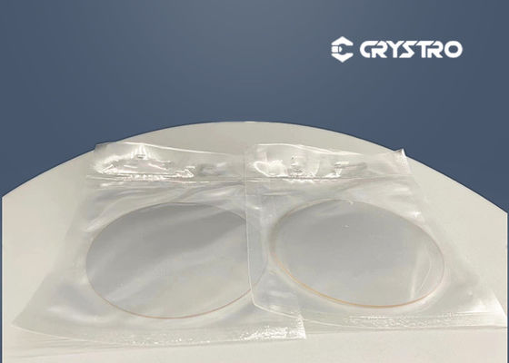
Each Single Crystal Substrate is carefully inspected and cleaned before packaging to ensure the highest quality standards are met. The substrates are individually placed in protective holders or trays to prevent any damage during handling and transportation.
For shipping, the substrates are securely packed in anti-static, cushioned containers designed to absorb shocks and vibrations. The packaging materials are chosen to protect against moisture, dust, and electrostatic discharge, preserving the integrity of the substrates throughout transit.
All shipments include detailed documentation, such as product specifications, handling instructions, and certificates of quality. We offer various shipping options to accommodate customer requirements, ensuring timely and safe delivery worldwide.
Please handle the packages with care upon receipt to maintain the pristine condition of the Single Crystal Substrates.
| Brand Name: | Crystro |
| Model Number: | SGGG |
Our Single Crystal Substrates are precision-engineered to meet the highest standards in advanced material applications, offering exceptional quality and performance. Designed specifically for use in cutting-edge technologies, these substrates serve as a fundamental platform for semiconductor, electronic, and optical devices. With a dielectric constant of 30, these substrates provide excellent electrical insulation properties, making them ideal for high-frequency and microwave applications where stable dielectric behavior is crucial.
Available in a cubic or round type, our Single Crystal Substrates cater to a wide range of industry needs. The cubic shape is especially suited for applications requiring precise orientation and uniform properties, while the round type substrate ensures compatibility with various fabrication processes and equipment. Both types are meticulously crafted to maintain uniformity and consistency, which is essential for achieving reliable device performance.
One of the standout features of our Single Crystal Substrates is their maximum size of up to 4 inch diameter, offering ample surface area for large-scale device fabrication. The 4inch diameter size is a perfect balance between manageable handling and sufficient working area, facilitating efficient processing and integration into complex device architectures. This size specification makes our substrates highly versatile and compatible with a wide range of semiconductor manufacturing tools.
To ensure superior surface quality and readiness for immediate use, our substrates are available with either EPI polished or double polished finishes. The EPI polished option is specifically designed to be EPI ready, meaning it is perfectly prepared for epitaxial layer growth without the need for additional surface treatment. This feature significantly streamlines the manufacturing workflow, reducing processing time and enhancing overall production efficiency. The double polished finish provides an ultra-smooth surface on both sides, ideal for applications that demand minimal surface defects and exceptional optical clarity.
Our Single Crystal Substrates also serve as excellent magneto-optical substrates, making them indispensable in the development of advanced optical devices that rely on magneto-optical effects. This characteristic is particularly beneficial for applications in optical isolators, modulators, and sensors, where precise control of light polarization and propagation is required. The intrinsic properties of these substrates enable enhanced performance and reliability in such specialized devices.
To guarantee the highest quality and compliance with industry standards, each batch of our Single Crystal Substrates comes with a comprehensive test report. This documentation provides detailed information on the substrate's physical, chemical, and electrical properties, ensuring that customers receive products that meet their stringent specifications. The test report serves as a valuable assurance of quality, facilitating trust and confidence in the use of our substrates for critical applications.
In summary, our Single Crystal Substrates combine a high dielectric constant of 30, versatile cubic and round types, and a convenient 4inch diameter size with superior polishing options including EPI polished and double polished finishes. Their magneto-optical substrate capabilities further expand their application scope, making them a preferred choice for researchers and manufacturers alike. With provided test reports and EPI ready surfaces, these substrates are ready to support the most demanding semiconductor and optical device fabrication processes, ensuring optimal performance and reliability.
| Polish | EPI Polished Or Double Polished (YSGG, Ra≤1nm, 3inch diameter) |
| Chemical Formula | Substituted GGG |
| Length Tolerance | ±0.2mm |
| Thermal Conductivity | 7.4 W·m⁻¹·K⁻¹ |
| Lattice Constant | 12.497 ± 0.003 Å |
| Dielectric Constant | 30 |
| Angle Direction | Customized |
| Mineralogical | Garnet |
| Thickness | 0.5 Or 0.63 mm |
| Type | Cubic / Round |
The Crystro Single Crystal Substrates, model number SGGG, originating from China, are precision-engineered materials designed to meet the rigorous demands of advanced scientific and industrial applications. With a maximum size of 4 inch diameter and a thickness option of 0.5 or 0.63 mm, these substrates offer exceptional structural integrity and uniformity, making them ideal for various high-precision uses.
One of the primary application occasions for the Crystro SGGG substrates is in the fabrication of epitaxial (EPI ready) thin films. Their excellent lattice constant of 12.497 ± 0.003 Å ensures minimal lattice mismatch, which is crucial for the growth of high-quality epitaxial layers. Researchers and manufacturers rely on these substrates for developing advanced semiconductor devices, optical coatings, and other high-performance electronic components where perfect crystal orientation and surface quality are indispensable.
Moreover, the Crystro SGGG substrates serve as superior magneto-optical substrates, making them highly suitable for applications in magneto-optical devices, sensors, and isolators. Their substituted GGG chemical formula enhances their magneto-optical properties, enabling improved performance in devices that require precise control of light and magnetic interactions. This makes them a preferred choice in fields such as telecommunications, data storage, and quantum computing.
In addition to research laboratories and semiconductor manufacturing, these single crystal substrates are widely used in optoelectronic device production, laser technology, and integrated photonic circuits. The availability of a comprehensive test report with each substrate guarantees their quality and consistency, providing confidence to users in critical applications.
Overall, Crystro’s SGGG single crystal substrates combine exceptional material quality with precise dimensional parameters, making them an indispensable component in the advancement of epitaxial film growth technologies and magneto-optical applications. Their EPI ready surface and reliable chemical composition contribute significantly to innovations in modern electronics and photonics industries.
Crystro offers premium Single Crystal Substrates, model number SGGG, originating from China. These substrates are made from high-quality garnet mineralogical material, featuring a cubic/round type structure with a diameter of up to 4 inches.
Designed specifically as substrate materials for YIG, the SGGG substrates support epitaxial growth of YIG and BIG films with excellent thermal conductivity of 7.4 W·m⁻¹·K⁻¹. The standard thickness available is 0.5mm, optimized for precise and reliable thin film applications.
Our product customization services allow you to tailor the Single Crystal Substrates to your exact specifications, ensuring compatibility and superior performance for your epitaxial growth processes. Whether you require specific dimensions or particular surface finishes, Crystro’s SGGG substrates provide the perfect foundation for advanced research and industrial applications.
Our Single Crystal Substrates product line is supported by a dedicated technical support team committed to providing comprehensive assistance throughout the product lifecycle. We offer expert guidance on substrate selection, handling, and application to ensure optimal performance in your specific use case.
Technical support services include detailed product specifications, material properties consultation, and troubleshooting assistance to address any challenges encountered during integration or processing. We also provide customized solutions tailored to unique project requirements, ensuring compatibility and enhanced functionality.
In addition to direct technical support, we offer a range of services such as substrate polishing, orientation customization, and quality assurance testing. Our state-of-the-art facilities enable precise control over crystal quality and dimensions, meeting the stringent demands of advanced semiconductor and optoelectronic applications.
We are committed to continuous improvement and innovation, working closely with customers to incorporate feedback and develop next-generation substrate materials. Our goal is to support your success by delivering reliable, high-quality single crystal substrates backed by responsive and knowledgeable service.
Each Single Crystal Substrate is carefully inspected and cleaned before packaging to ensure the highest quality standards are met. The substrates are individually placed in protective holders or trays to prevent any damage during handling and transportation.
For shipping, the substrates are securely packed in anti-static, cushioned containers designed to absorb shocks and vibrations. The packaging materials are chosen to protect against moisture, dust, and electrostatic discharge, preserving the integrity of the substrates throughout transit.
All shipments include detailed documentation, such as product specifications, handling instructions, and certificates of quality. We offer various shipping options to accommodate customer requirements, ensuring timely and safe delivery worldwide.
Please handle the packages with care upon receipt to maintain the pristine condition of the Single Crystal Substrates.